SILICON TECHNOLOGY SIMULATION
Developing a silicon technology is a capital intensive
enterprise. A new fabrication facility ("fab") can cost as much as a
billion dollars. To recoup that investment, it is imperative
that a new fab begin generating product as rapidly
as possible, and that there be a minimimum of trial and error
employed in developing viable processes in that fab.
Therefore it is extremely useful to have computer simulation tools which
can predict, before the processing of any samples or the manufacturing of
any product, what the performance of a technology will be, and how
to optimize that performance by adjusting the engineering controls available,
such as furnace temperatures, gas flows, and implantation doses.
Several tools have been developed for this purpose.
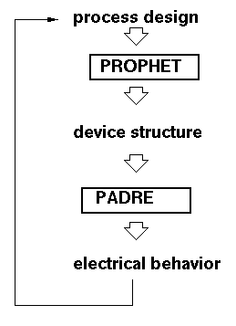 The simulator
PROPHET
is a process simulator, which predicts the outcome of
process parameters on transistor structure.
The simulator
PADRE
is a device simulator, which reads a description of a transistor
structure and predicts its electrical behavior.
The simulator
PROPHET
is a process simulator, which predicts the outcome of
process parameters on transistor structure.
The simulator
PADRE
is a device simulator, which reads a description of a transistor
structure and predicts its electrical behavior.
Used in conjunction, the two tools can predict transistor behavior
long before the availability of experimental data.
As a result, a circuit designer can begin circuit and
system design today, using numbers derived from simulation,
for a technology which will not exist for
another 18 months or two years.
The advantages of such a predictive capability should be evident.
The time-to-market is greatly reduced. Development cost in the fab
can be slashed by eliminating many trials; instead that same
fab time can be used fabricating product.
Simulation can be used to analyze process sensitivity, to design
viable processes which are far away from "cliffs" in parameter space.
It can be even be used to examine new transistors or device ideas
for which no known fabrication method exists yet; the simulations
help decide the value of allocating resources to such new directions.
One measure of the usefulness of simulation is that in Lucent
fabs, simulators are accessed about 10,000 times a month, or
approximately once a minute through the working day.
In the following sections, process and device simulation is
described in more detail. Thumbnail graphics are included
in the text; any picture can be magnified by clicking on it.
|
SIMULATION OF SILICON PROCESSING
|
Silicon chips are prepared by an elaborate sequence of
processing steps applied to a silicon wafer. The most common
processing steps are the deposition and patterning of insulating or
metallic layers, the implantation of impurities to convert the
neutral crystal into a positive (p-type) or negative (n-type)
conductor, and heat treatment to anneal crystal damage or grow
insulating oxide.
The development of a process which leads to a circuit of desired
performance involves many decisions on processing conditions at
each step in the process sequence. Traditionally such decisions
have been made by trial and error. The goal of technology
simulation is to develop computer simulation tools to predict
the outcome of process steps, and thereby reduce the guesswork
in developing a process sequence.
Each process step involves a series of physical and chemical
modifications of the wafer surface and subsurface. Simulation
of these steps is handled by the solution of differential
equations for mass transport and material flow in the bulk, and
by ballistic transport techniques on the surface.
The following sequence of pictures illustrates some of the steps
which can be simulated in silicon processing.
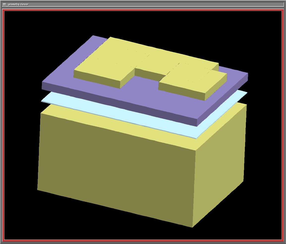
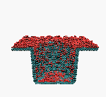
FILM DEPOSITION AND PATTERNING
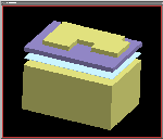 A thin oxide buffer layer is deposited on the wafer,
followed by hard silicon nitride layer. The nitride acts as a mask for a
subsequent oxidation process. The nitride in turn is covered by
an organic photosensitive layer which is patterned by a
photographic process. The pattern will then be transferred into
the nitride by exposing the wafer to plasma chemistry which
etches the nitride without attacking the photoresist.
Finally the photoresist is removed by a different solvent, leaving patterned
nitride. In the figure, the layers are shown exploded for illustration.
A thin oxide buffer layer is deposited on the wafer,
followed by hard silicon nitride layer. The nitride acts as a mask for a
subsequent oxidation process. The nitride in turn is covered by
an organic photosensitive layer which is patterned by a
photographic process. The pattern will then be transferred into
the nitride by exposing the wafer to plasma chemistry which
etches the nitride without attacking the photoresist.
Finally the photoresist is removed by a different solvent, leaving patterned
nitride. In the figure, the layers are shown exploded for illustration.
|
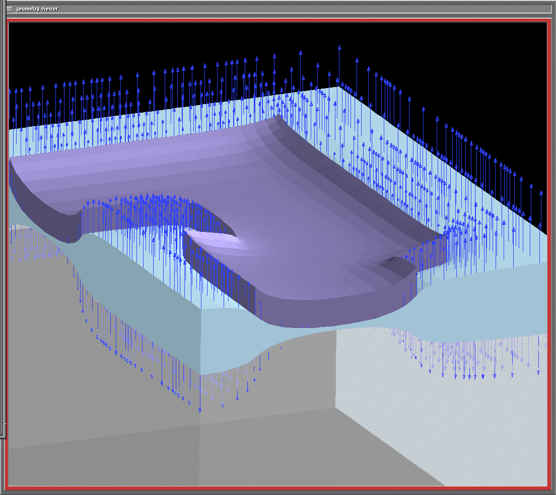
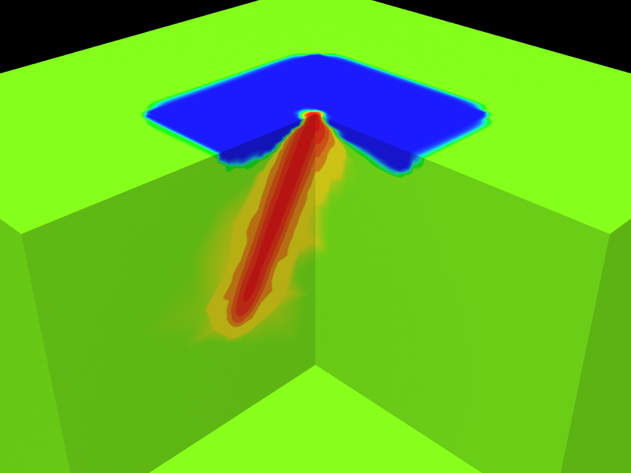
SILICON OXIDATION
 To separate conducting areas from one another, a layer of
insulating dioxide is grown. The oxide is grown by exposing the
silicon surface to high temperature steam. As the oxide grows,
the silicon is consumed. The arrows represent the direction of
motion of each surface of the oxide. Underneath the nitride
mask, the growth is suppressed, and these areas will become the
active transistor area. Where the arrows are longest, the oxide
is growing rapidly, and these areas become the isolation between
transistors.
To separate conducting areas from one another, a layer of
insulating dioxide is grown. The oxide is grown by exposing the
silicon surface to high temperature steam. As the oxide grows,
the silicon is consumed. The arrows represent the direction of
motion of each surface of the oxide. Underneath the nitride
mask, the growth is suppressed, and these areas will become the
active transistor area. Where the arrows are longest, the oxide
is growing rapidly, and these areas become the isolation between
transistors.
|
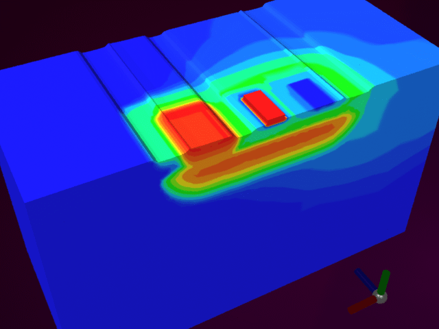
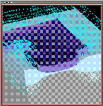
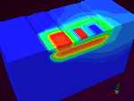
ION IMPLANTATION
 The neutral silicon is converted to a negative or positive
conductor by the process of ion implantation. Dopant atoms
are ionized and then accelerated by an electric field until they
impinge on the silicon surface, where they embed themselves.
During subsequent thermal treatment, the dopants redistribute.
The concentration of dopant atoms at any point determines the
electrical properties of the crystal at that point. Process
simulation is used here to predict the contours of phosphorus
concentration in the silicon. A polysilicon line crosses the
active area in the upper left and forms the gate of a
transistor.
The neutral silicon is converted to a negative or positive
conductor by the process of ion implantation. Dopant atoms
are ionized and then accelerated by an electric field until they
impinge on the silicon surface, where they embed themselves.
During subsequent thermal treatment, the dopants redistribute.
The concentration of dopant atoms at any point determines the
electrical properties of the crystal at that point. Process
simulation is used here to predict the contours of phosphorus
concentration in the silicon. A polysilicon line crosses the
active area in the upper left and forms the gate of a
transistor.
|
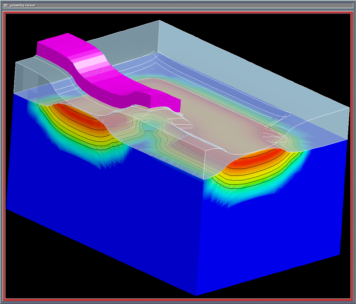
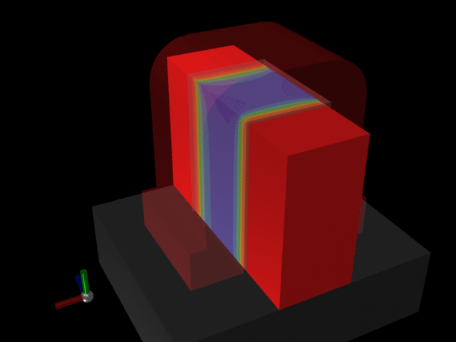
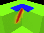
METALLIZATION
 After the transistors are built in the silicon, they must be
interconnected using metal layers above the silicon substrate.
First an insulating glass layer is deposited to cover the
silicon, then contact holes are cut into the glass layer down to
the silicon. Metal is deposited on top of the glass, connecting
to the devices through the contact holes. Process simulation can be
used to predict the hole filling capabilities of different metal
deposition techniques. The graphic shows a snapshot during the
filling of a contact hole with aluminum.
After the transistors are built in the silicon, they must be
interconnected using metal layers above the silicon substrate.
First an insulating glass layer is deposited to cover the
silicon, then contact holes are cut into the glass layer down to
the silicon. Metal is deposited on top of the glass, connecting
to the devices through the contact holes. Process simulation can be
used to predict the hole filling capabilities of different metal
deposition techniques. The graphic shows a snapshot during the
filling of a contact hole with aluminum.
|
|
SIMULATION OF SILICON DEVICES
|
Device simulation is used to predict the electrical behavior of
a transistor, or other semiconductor device, from its
structure.
Device simulation often follows process simulation, which
predicts the structure of a device. Used in this way, it allows
a designer to choose the process inputs which result in the
desired device parameters, such as on-current, off-current and
threshold voltage.
However device simulation can also be applied to structures for
which no known fabrication method exists. In this mode,
simulation is used to explore new inventions in device design;
if the new device is interesting, methods of fabricating it can
then be explored.
Device simulation is also widely used to understand unexpected
device behavior, by providing a detailed picture of the internal
electric fields and carrier distribution when voltages are
applied to the device.
Device simulation is carried out either by solving a set of
differential equations decribing the electric fields and
carrier populations in the device, or by following the motion of
a representative set of individual particles.
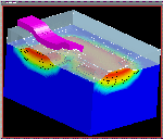
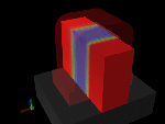
BIPOLAR TRANSISTOR GAIN
 A bipolar transistor used in Lucent's 0.9um process is simulated here.
Device simulation was used to understand the surprisingly large
gain of the device when operated in reverse mode. The collector
is at left, the emitter at center and base at right.
A bipolar transistor used in Lucent's 0.9um process is simulated here.
Device simulation was used to understand the surprisingly large
gain of the device when operated in reverse mode. The collector
is at left, the emitter at center and base at right.
|
ALPHA PARTICLE STRIKE
 Alpha particle strikes from cosmic rays are a significant source
of leakage for charge stored in memory cells. The disturbance
caused by an alpha particle strike is simulated here; the
particle enters at the surface and causes ionization in its
wake.
Alpha particle strikes from cosmic rays are a significant source
of leakage for charge stored in memory cells. The disturbance
caused by an alpha particle strike is simulated here; the
particle enters at the surface and causes ionization in its
wake.
|
DELTA TRANSISTOR
 An efficient transistor can be formed by wrapping a gate
around a silicon pedestal. The gate here, represented as
transparent, induces carriers between the source and drain,
allowing current to flow. Although no reliable fabrication methods
are yet known for this device, it may become significant in future
generations of technology.
An efficient transistor can be formed by wrapping a gate
around a silicon pedestal. The gate here, represented as
transparent, induces carriers between the source and drain,
allowing current to flow. Although no reliable fabrication methods
are yet known for this device, it may become significant in future
generations of technology.
|
SILICON BAND STRUCTURE
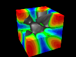 To follow the motion of energetic carriers, a detailed picture
of the silicon band structure is required. This figure shows
the first Brillouin zone of silicon, and illustrates the strong
influence of the crystallographic axes on the motion of
carriers.
To follow the motion of energetic carriers, a detailed picture
of the silicon band structure is required. This figure shows
the first Brillouin zone of silicon, and illustrates the strong
influence of the crystallographic axes on the motion of
carriers.
|
More information
Movies!
This MPEG movie (1.2M) illustrates a full process flow,
stepping through each of the process modules which would be used in a typical
modern process. Click here.
This MPEG movie (5.2M) shows the detailed interaction
of point defects and impurities during the anneal of crystal damage
caused by ion implantation.
As the damage is removed during furnace is annealing, the previously
implanted impurities are redistributed.
Click here.
Page author csr